Contact

ADA-SDEV-KIT2

Summary

The ADA-SDEV-KIT2 has been replaced by the ADA-SDEV-KIT3. For the latest specification please visit the ADA-SDEV-KIT3 webpage.

The ADA-SDEV-KIT2 is a Development Kit for the Xilinx Radiation Tolerant Kintex Ultrascale XQRKU060 Space-Grade FPGA.

Modular design with Industrial XCKU060 in -1 speed grade, XRTC compatible Configuration Module, two FMC Sites, DDR3 DRAM, System Monitoring and reference Space-Grade Power and Temperature Sensing solutions from Texas Instruments.
See http://www.ti.com/tool/ALPHA-XILINX-KU060-SPACE for further details.

Applications

Kintex UltraScale Space Development Kit

Board Features

ADM-SDEV-BASE - FPGA Board
ADM-SDEV-CFG - XRTC Configuration FMC
Space-Grade Power and Temperature Sensing solutions from Texas Instruments
FMC+ HPC Interface
FMC LPC Interface
XRTC Compatible Configuration FMC Interface
SODIMM Memory Socket (8GB Fitted)

FPGA Features (Hard IP)

3x PCI Express Gen3 cores

Specification

Board Format

Development Platform
Width: 165 mm
Depth: 225 mm
Weight: Without Heatsink 290 g

Environmental Specifications

Temperature Limits
Operating Temperature RangeStorage Temperature Range
MinMaxMinMax
AC0Air Cooled Commercial0°C+55°C-40°C+85°C

Operating Humidity Range:
Up to 95% (non-condensing)


Host I/F

n/a


Target Device

Xilinx Kintex® UltraScale™
XCKU060-1-I, XQRKU060-(CA1509) (1FFVA1517)

FPGA Resources

Chosen DeviceFFsLUTsDSPsBRAM
XCKU060-1-I663k221k276038.0Mb
XQRKU060-(CA1509)663k221k276038.0Mb

FPGA Hard IP Cores

3x PCI Express Gen3 cores

On Board Memory

Memory TypeNo. BanksMemory Size (per bank)
SODIMMs11G x 72 (8GiB) DDR3-1600

Target FPGA Configuration

configured by XRTC compatible Configuration FMC or through JTAG socket on the Configuration FMC


FPGA Configuration Flash

Flash TypeFlash Size
QSPI2x256MB

I/O Interfaces

Interface TypeQtyDescription
ON-BOARD I/O (FMC+ Socket)
FMC+ HPC Interface24High-speed Serial IO
FMC+ HPC Interface160/80Single Ended/Differential Pair I/O
ON-BOARD I/O (FMC LPC Socket)
FMC LPC Interface4High-speed Serial IO
FMC LPC Interface68/34Single Ended/Differential Pair I/O
ON-BOARD I/O (FMC mounted IPASS Connector)
XRTC Compatible Configuration FMC Interface1PCI Express x1 Interface
ON-BOARD I/O (FMC mounted USB Connector)
XRTC Compatible Configuration FMC Interface1USB Interface
ON-BOARD I/O (FMC mounted SATA Connectors)
XRTC Compatible Configuration FMC Interface2SATA Interfaces
ON-BOARD I/O (Commercial Grade QSPI flash for power on configuration)
XRTC Compatible Configuration FMC Interface1QSPI Flash Interface

Ordering Information

Ordering Code
ADA-SDEV-KIT2/C
NoteThis is the Rev2 assembly, contact sales for other configuration options.
For rev1 (ADA-SDEV-KIT) pricing and availability contact sales.

Related Products

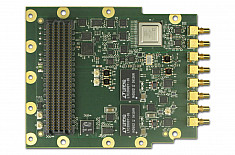
FMC-DA4

FMC-DA4

RF/IF Signal Sampling/Generation

The FMC-DA4 is an FMC I/O Module, providing two Analog to Digital converters with 14-bit resolution and sampling rates up to 3Gsps, and two Digital to Analog converters with 16-bit resolution and sampling rates up to 2.7Gsps.

View Product

FMC-RCP-10G

FMC-RCP-10G

40G Ethernet

The FMC-RCP-10G is an FMC I/O Module with up to four 10Gb/s Optical transceiver channels.

View Product

FMC-RCP-4G

FMC-RCP-4G

High-Speed Communications

The FMC-RCP-4G is an FMC I/O module with up to four 4Gb/s Optical transceiver channels.

View Product

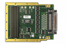
FMC-IO68

FMC-IO68

Discrete I/O

The FMC-IO68 is an FMC I/O Module which provides a discrete I/O Interface.

View Product

FMC-CAMERALINK

FMC-CAMERALINK

Camera Link I/O Interface

The FMC-CAMERALINK is an FMC I/O Module which provides an industry standard CameraLink interface.

View Product

FMC-IPASS

FMC-IPASS

PCI Express Gen 3 Interface

The FMC-IPASS is an FMC I/O Module which provides an industry standard High-Speed Serial interface.

View Product

Resources:

Product Change Notices

PCN-202101-1.0

Reference Designs: (RD-SDEV)

The RD-SDEV contains a suite of Vivado reference designs demonstrating how to use the board, including PCIe DMA examples, DDR4 memory examples, and GT IBERT example. The ADA-SDEV-KIT2 also uses the RD-SDEV reference designs.

PCIe examples are compatible with the ADXDMA Driver and API.

Download Reference Designs [Login Required]

Download the ADXDMA Driver [Login Required]


Deliverables

ADA-SDEV-KIT2 Board
One-Year Warranty
One-Year Technical Support
Example Vivado Projects
Reference Schematics Available

ADA-SDEV-KIT2 Deliverables:

HardwareADM-SDEV-BASE - XCKU060-1I FPGA board
ADM-SDEV-CFG - XRTC Compatible FMC configuration board
DocumentationADM-SDEV-BASE User Manual
ADM-SDEV-CFG User Manual
ADA-SDEV-KIT Programming Guide
ADM-SDEV-BASE Schematics (PDF)
ADM-SDEV-CFG Schematics (PDF)
ADM-SDEV-BASE Bill of Materials (EXCEL format)
ADM-SDEV-BASE PCB Layout files (Cadence Allegro format)
FirmwareXilinx Constraints Files
Example DDR3 Memory SDK project
Example GPIO, IBERT and Clock Test projects
SoftwareAVR2UTIL.EXE - remote access FPGA board status monitoring utility

Additional Resources Required:

HardwareATX power supply - 24pin ATX12V 2.X (min 100W on +5V rail)
Xilinx Platform Cable USB II - https://www.xilinx.com/products/boards-and-kits/hw-usb-ii-g.html
USB Cable (to fit onboard Micro-USB AB connector) for remote monitoring using AVR2UTIL.EXE utility (requires separate PC to run software on)
SoftwareXilinx Vivado Design Suite - 2018.1 or later

Support

Please contact Alpha Data for full details on the available support packages for the ADA-SDEV-KIT2.

Sales Questions

Sales Questions

For any sales questions please e-mail us at sales@alpha-data.com

Sales Questions

Technical Support

For any technical questions please e-mail us at support@alpha-data.com

Get in touch and request a quote


Contact Us